Documentation
- First draft of SPD Router specification. (PDF format)
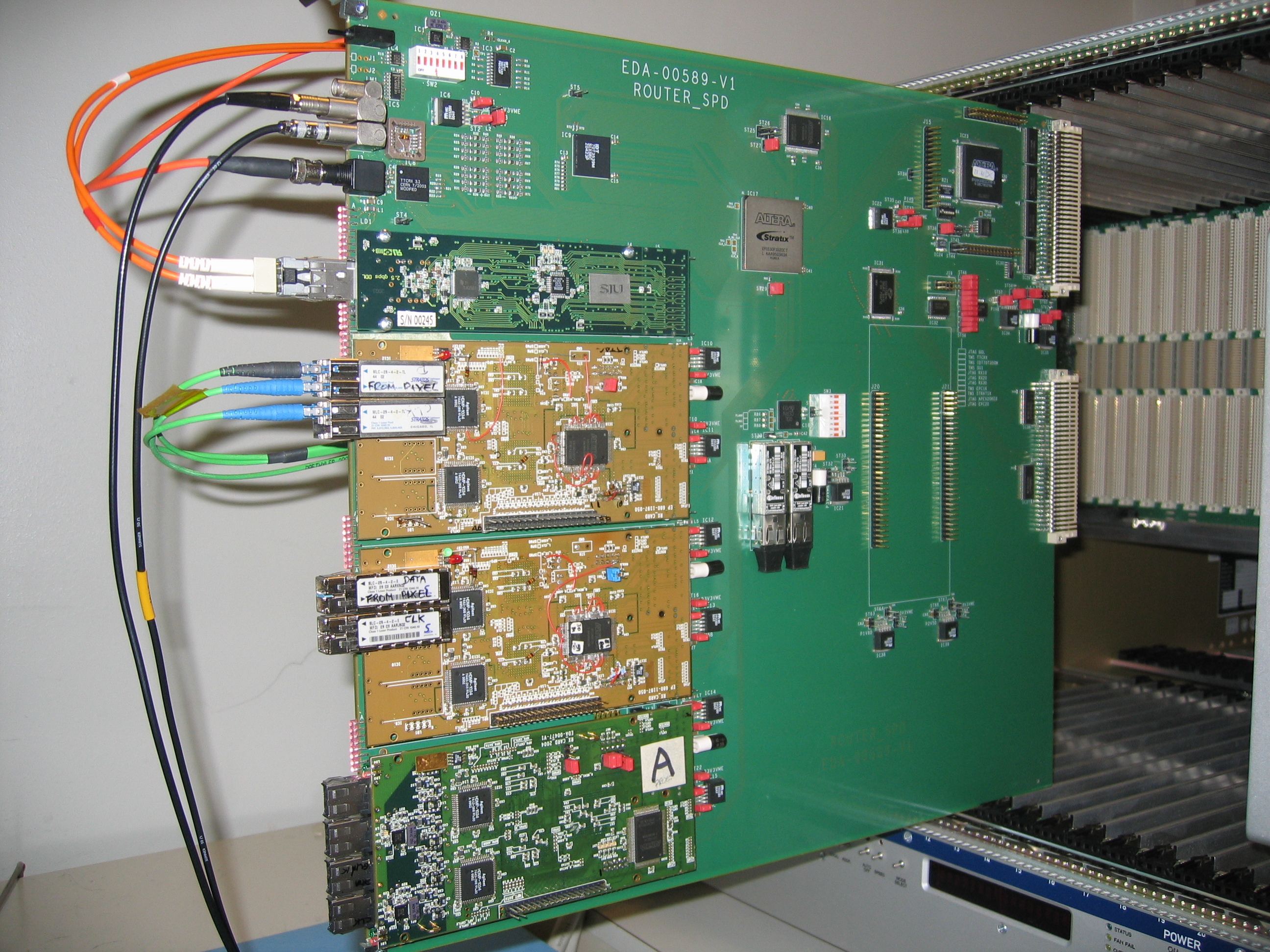
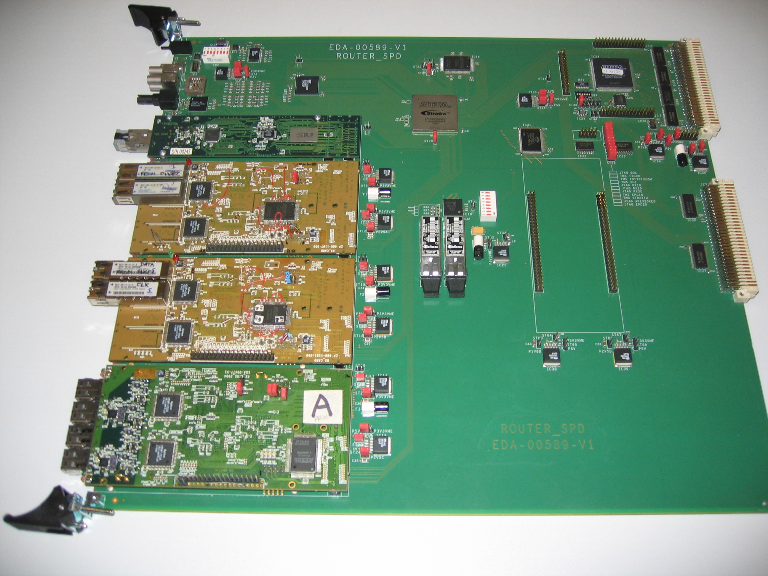
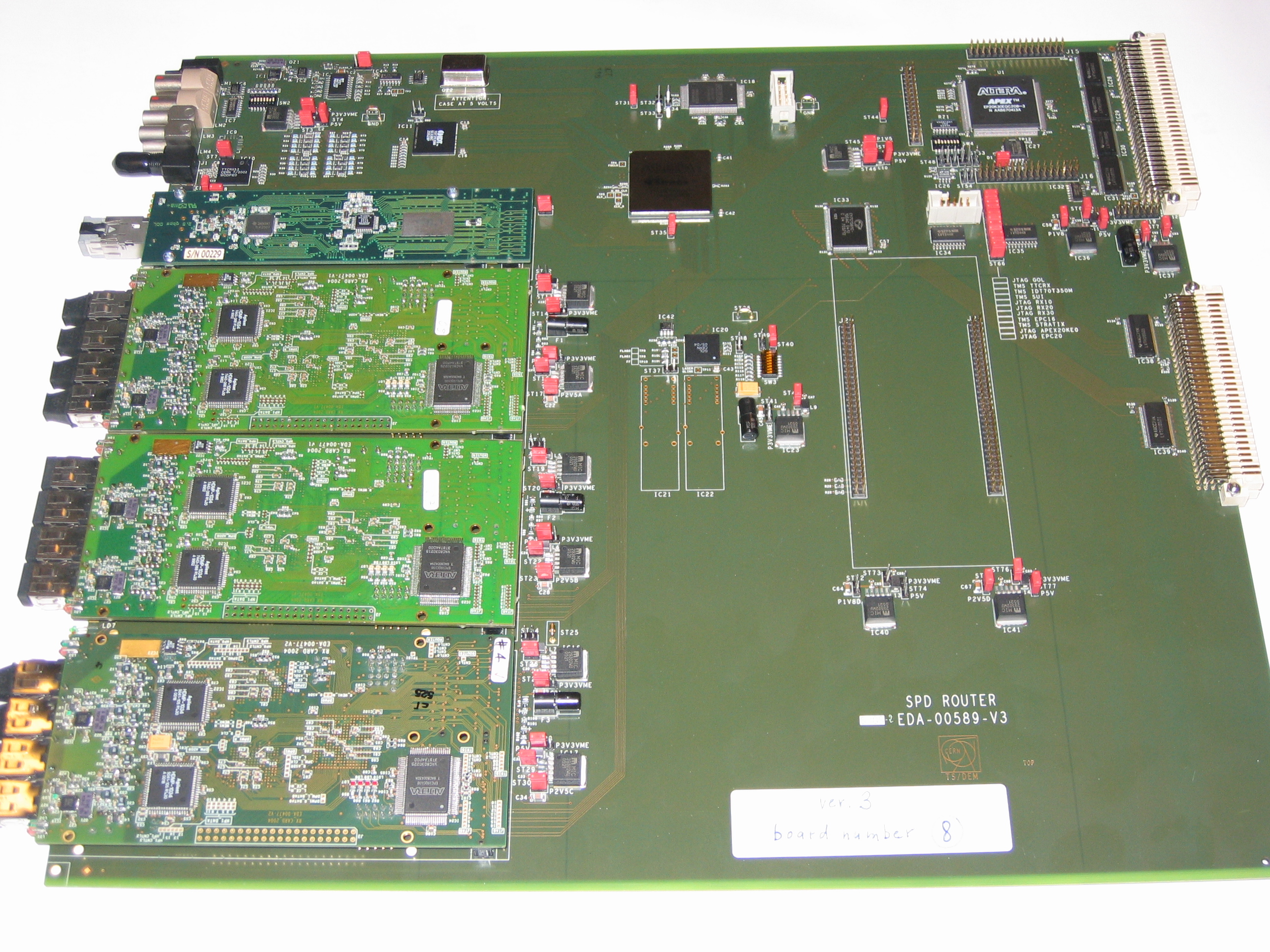
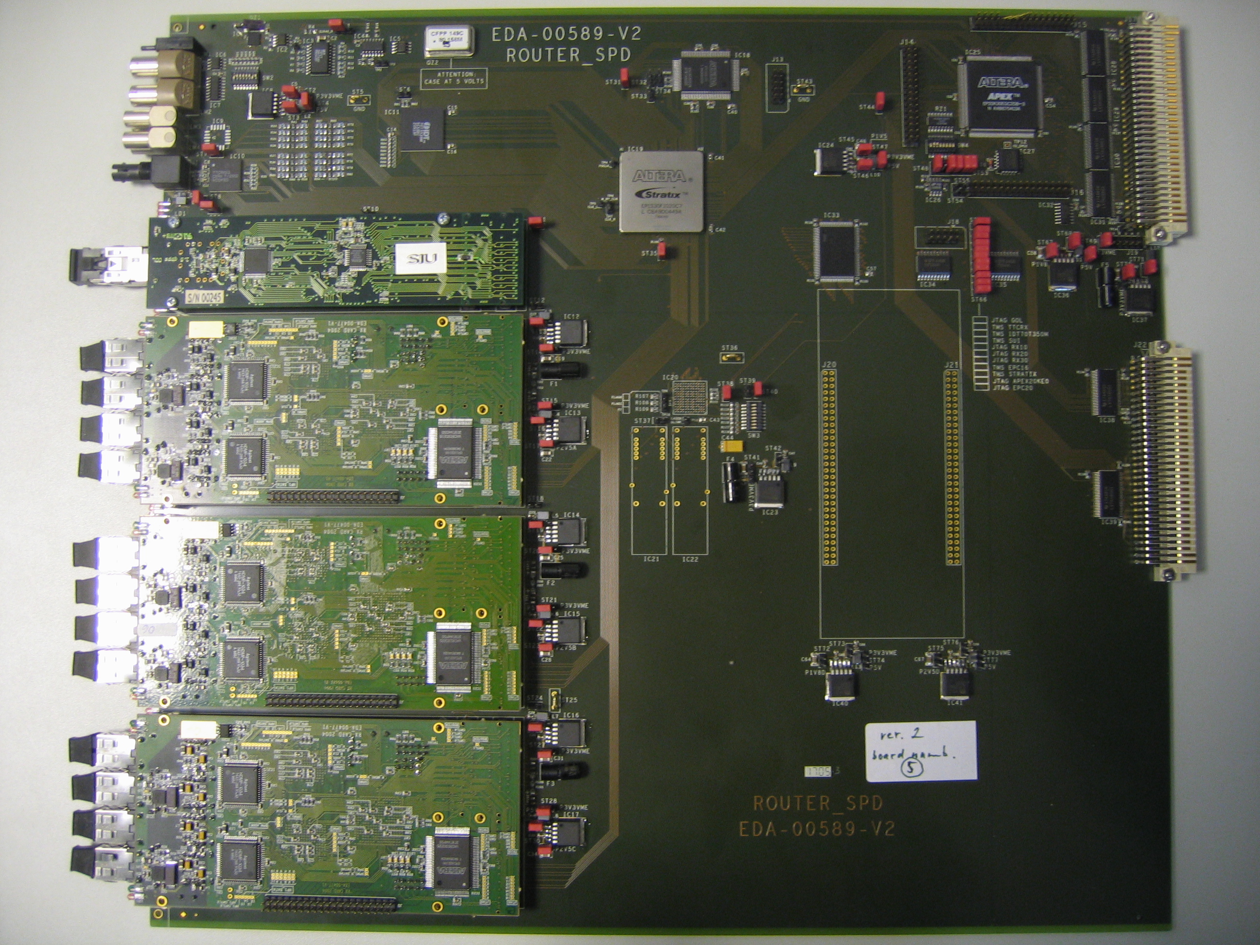
- Schematics capture (EDA-00589-V3 EDA-00589-V2 EDA-00589_V1), for LinkReceiver (EDA-00477-V2_sch)
- PCB layout (EDA-00589-V3 EDA-00589-V2 EDA-00589_V1), for LinkReceiver (EDA-00477-V2_pcb)
- Front Panel (EDA-00589-V3)
- Allocation of SPD Routers in 2 6U/9U VME crates (boards_allocation_in_9UVMEcrate.ppt)
- Pinout for router_fpga (router_fpga_v123.xls)
- Pinout for vme_fpga (vme_fpga_v123.xls)
- LECC_2006_presentation.ppt, LECC_2006_proceedings.pdf
- SPD Router registers (update 04/12/2014 Ver 37)
- JAM_file_instructions.pdf ( router_fpga_jamplayer_sof.cdf router_fpga_jamplayer_pof.cdf )
- LinkRx registers
- VME address space
Programming Files
- Router_fpga ver.1 (JAM file) - first version
- Router_fpga ver.2 (JAM file) - added temp interlock functionality
- Router_fpga ver.3 (JAM file) - improved address counter for 6 channels
- Router_fpga ver.4 (JAM file) - added BUSY from vme bus (control reg), delay for sequencer is set to 400us
- Router_fpga ver.5 (JAM file) - improved start address fifo
- Router_fpga ver.6 (JAM file) - added fast-or functionality
- Router_fpga ver.7 + LinkRx_fpga ver.6- resets for fifo_start_address and fifo_end_address replaced by flash_dpm, improved Verilog code for output from fifos (for Quartus !), improved state machine for decoding L0 and L1 from TTCrx chip
- Router_fpga ver.8 + LinkRx_fpga ver.6 - improved state machine for L2_message, added bit "exclude triggers from TTC" to control register, added fifo(max.32 words) for router_header and info about router_header present is in DAQ header WORD3 bit[30]
- Router_fpga ver.9 + LinkRx_fpga ver.7 - improved router header functionality (first word in router header is length of router header) and temp_limit set to hex 247 for MCM and hex 2f2 for BUS, changed comparison temp_limit for MCM (negative behavior of resistance !!!)
- Router_fpga ver.10 + LinkRx_fpga ver.8 - (new chain: JAM for FPGAs, JAM for FLASHs) - separate reset for temp_limit registers, changed bit orded for receiving L1 message, improved fastor functionality (Indications bus 3,4,5) inside LinkRx
- Router_fpga ver.11 + LinkRx_fpga ver.9 - improved timing for BCNT from TTCrx chip with second clock moved by 14 ns, implemented PLL, improved l1_fifo, l2_fifo, bcnt_on_ttcrx_fifo, created ttc_input_fifo, added condition for: router_busy <= n_of_triggers_in_l1_fifo >= 30 , improved counter for fastor and added 6 bits to control register(bits for disable fastor)
- Router_fpga ver.12 + LinkRx_fpga ver.10 - improved led indication for a front panel, implemented data format error check state machine, implemented separate reset for router header fifo
- Router_fpga ver.13 + LinkRx_fpga ver.13 - added led indication for idle_violation and busy_violation, added SEU error to status register, improved Verilog code in slm_check.v, improved temp_reading state machine - added 4 wait cycles (4 wait cycles for wait for end of readout), improved DDL_fifo, added into state check_other_processes of master_state_machine wire read_temp_check
- Router_fpga ver.14 + LinkRx_fpga ver.14 - added functionality for FastOR, implemented state machine for trigger sequence monitoring
- Router_fpga ver.15 + LinkRx_fpga ver.15 - added serializer of 16 status registers in linkRx and deserializer of the 16 status registers of linkRx in the Router (used redundant 6 P_TRST pins for each channel) between Router and linkRx, added vme access to 6 x 16 = 96 registers, vme addresses are from hex 80 to hex df
- Router_fpga ver.16 + LinkRx_fpga ver.16 - improved data_error_checking state machine to check also chip number and event number in the header word
- Router_fpga ver.17 + LinkRx_fpga ver.16 - router busy output signal is active in 1 (before was active in 0), changed time for reset_gol to 10 us
- Router_fpga ver.18 + LinkRx_fpga ver.16 - reset_for_FEE from TTC system implemented i.e. reset in the same time for all Routers
- Router_fpga ver.19 + LinkRx_fpga ver.17 - synchronization of phase of 10MHz clock implemented (this clock is used to send commands on Trig_data bus), reset_for_FEE is also sent to Trig_rst_N pin, which is common for 3 linRx, inside linkRx reset_for_FEE is doing reset of ROB
- Router_fpga ver.20 + LinkRx_fpga ver.17 - added options for scope 0, 1, 2 , added counters for fastor_linkrx1, fastor_linkrx2, fastor_linkrx3, fastor_mormal, fastor_coincidence (all these counters are time counters), added programmable register time_for_fastor_counter
- Router_fpga ver.21 + LinkRx_fpga ver.17 - added functionality to clean fake fastor pulse after L2y, new registers: status0_reg_linkRx_ch0, status1_reg_linkRx_ch0, status2_reg_linkRx_ch0, status3_reg_linkRx_ch0, status4_reg_linkRx_ch0, status5_reg_linkRx_ch0, status6_reg_linkRx_ch0, status7_reg_linkRx_ch0, status8_reg_linkRx_ch0, status9_reg_linkRx_ch0, status10_reg_linkRx_ch0, status11_reg_linkRx_ch0, status12_reg_linkRx_ch0, status13_reg_linkRx_ch0, status14_reg_linkRx_ch0, status15_reg_linkRx_ch0, and the same type of status registers for channels 1, 2, 3, 4, 5
- Router_fpga ver.22 + LinkRx_fpga ver.17 - added ttcrx not ready state to BUSY state, improved state machine for checking trigger sequences
- Router_fpga ver.23 + LinkRx_fpga ver.17 - corrected bits for WORD_3 (participated sudetectors) in DAQ header
- Router_fpga ver.24 + LinkRx_fpga ver.17 - added qpll not locked state to BUSY state, improved master state machine - after data transfer from linkRx to DAQ there is check that DDL fifo is empty. Only after check that DDL fifo is empty, FEE status word is sent to DAQ
- Router_fpga ver.25 + LinkRx_fpga ver.1024 - added separate command for "reset_digital_pilot" (via RX40), added separate command for "reset_pixel", added separate command for "reset_pll", added decoding of PrePulse from TTC, added bit enable_PP_to_be_TP in router_control_reg, added reset_for_FEE to DDL_fifo in order to clear buffer at the beginning of each run, added bit "trigger_error" to WORD_4[24] to DAQ header, added bit "FEE_ERROR==linkRx_busy" to WORD_4[17] to DAQ header, changed n_of_l1_triggers <= 7, added 1 clk delay for data received from m_data_in (this is valid from linkRx_fpga_core_ver24 !!!), implemented Fast input registers inside FPGA for signals coming from TTCrx chip, implemented Fast input, output registers inside FPGA for signals going to LinkRxs, changed delay for clk1 to 16.4 ns, improved trigger_sequence_monitoring, added "l0_l1_time" register
- Router_fpga ver.26 + LinkRx_fpga ver.1124 - added R/W register timeout_for_event_ready(hex e30000) - after reset there is 300 (i.e. 300us), added R/W register number_of_l1_in_l1fifo(hex e40000) - after reset there is 7, changed in Busy_logic module: l0_timeout=(l0_timer==9'd250) - i.e. 6,25 us, for register "busy" changed priority to "set_busy"
- Router_fpga ver.27 + LinkRx_fpga ver.25 - changed bit "FEE_ERROR==linkRx_fatal_error" in WORD_4[17] in DAQ header
- Router_fpga ver.28 + LinkRx_fpga ver.26 - added states to master state machine for waiting data from linkRx before checking that DDL fifo is empty
- Router_fpga ver.29 + LinkRx_fpga ver.27 - changed functionality on Indication [5:0] to have channel_busy [5:0], added disable_channel for each channel_busy i.e. if channel is disabled than channel_busy for this channel is not active, added BusyResolver.v and RxLinkReady.v module
- Router_fpga ver.30 + LinkRx_fpga ver.27 - new L0_L1time==260 BCs after reset, for sending PrePulse TTC signal as Test Pulse for pixel chips, modification of the Trig_ENA signals (in det_interface.v module), added update of l2_fifo when the routers received a valid L2r from TTC (module TTC.v), Protection for L1_ fifo, Additional scope signals
- No entries found for versions 31-36 [GAR]
- No entries found for versions 31-36 [GAR]
- No entries found for versions 31-36 [GAR]
- No entries found for versions 31-36 [GAR]
- No entries found for versions 31-36 [GAR]
- No entries found for versions 31-36 [GAR]
- Router firmware revision for RUN2, Ver 37.
Compliant CDH (V3),
Trigger seqeunces error flags connected to CDH Status Error Field,
3 additional registers: s_time_l0_to_l1m[15:0], s_time_l0_to_l2m[17:0], s_cdh_status_error_mask[19:0]. [GAR]
Descriptions of changes for each version of LinkRx are here.
Production of SPD Routers
| BOARD NUMBER | DESCRIPTION |
|---|---|
| 1 | ver.1- Don't use this board as final board !!! |
| 2 | ver.1, corrected 2 wires on PCB (there was short circuit between them)- Don't use this board as final board !!! |
| 3 | ver.2 - production in Slovakia (ELPRO), does not work - wrong PCB and soldering of FBGA 1020 pins - DEAD !!! |
| 4 | ver.2 - production in Slovakia (ELPRO), does not work - wrong PCB and soldering of FBGA 1020 pins - DEAD !!! |
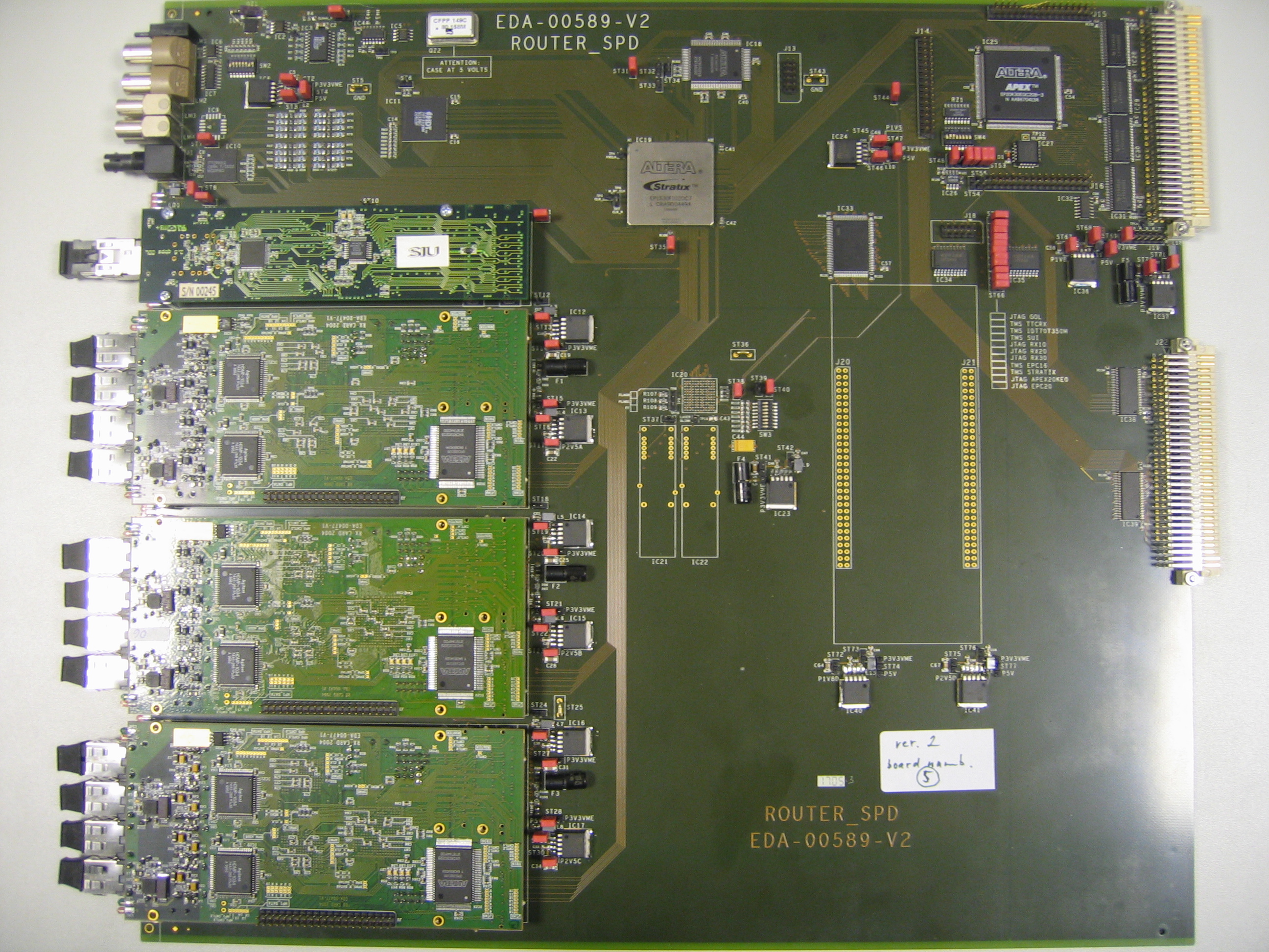
| 5 | ver. 2 - production in Barco and ACAMAS, modif. for crystal of QPLL, R230 is changed to jumper, wire to nconfig for power sequencing of Altera APEX 20KE - Don't use this board as final board !!! |
| 6 | ver. 2 - production in Barco and ACAMAS, modif. for crystal of QPLL, R230 is changed to jumper, wire to nconfig for power sequencing of Altera APEX 20KE- Don't use this board as final board !!! |
| 7 | ver. 2 - production in Barco and ACAMAS, modif. for crystal of QPLL, R230 is changed to jumper, wire to nconfig for power sequencing of Altera APEX 20KE- Don't use this board as final board !!! |
| 8 | ver. 3 - production in Barco and ACAMAS - final production - board o.k, but the board bent 2%, silkscreen for select ID is wrong !!! |
| 9 | ver. 3 - production in Barco and ACAMAS - final production - board o.k, but the board bent 2%, silkscreen for select ID is wrong !!! |
| 10 | ver. 3 - production in Barco and ACAMAS - final production - the board bent 2%, silkscreen for select ID is wrong, 6 missing connections !!! - connections between linkrx1,linkRx2 and linkRx3 are replaced by wires on the PCB - Don't use this board as final board !!! |
| 11 | ver. 3 - production in Barco and ACAMAS - final production - board o.k, but the board is not possible to plug in vme connectors (bentness 3mm) |
| 12 | ver. 3 - production in Barco and ACAMAS - final production - board o.k. |
| 13 | ver. 3 - production in Barco and ACAMAS - final production - board o.k. |
| 14 | ver. 3 - production in Barco and ACAMAS - final production - board o.k. |
| 15 | ver. 3 - production in Barco and ACAMAS - final production - board o.k. |
| 16 | ver. 3 - production in Barco and ACAMAS - final production - board o.k. |
| 17 | ver. 3 - production in Barco and ACAMAS - final production - board o.k. |
| 18 | ver. 3 - production in Barco and ACAMAS - final production - board o.k. |
| 19 | ver. 3 - production in Barco and ACAMAS - final production - board o.k. |
| 20 | ver. 3 - production in Barco and ACAMAS - final production - board o.k. |
| 21 | ver. 3 - production in Barco and ACAMAS - final production - board o.k. |
| 22 | ver. 3 - production in Barco and ACAMAS - final production - board o.k.. For proper behavior the board needs stong pressing into vme crate due to bent board. At P2 there was problem with 3-rd position for likRx. It must be checked !!! |
| 23 | ver. 3 - production in Barco and ACAMAS - final production - board o.k., but some components deformated by temperature during resoldering of FPGA 1020 pins |
| 24 | ver. 3 - production in Barco and ACAMAS - final production - board o.k. |
| 25 | ver. 3 - production in Barco and ACAMAS - final production - board o.k. |
| 26 | ver. 3 - production in Barco and ACAMAS - final production - board o.k. |
| 27 | ver. 3 - production in Barco and ACAMAS - final production - board o.k. |
| 28 | ver. 3 - production in Barco and ACAMAS - final production - board o.k. |
| 29 | ver. 3 - production in Barco and ACAMAS - finalproduction - board o.k. |
| 30 | ver. 3 - production in Barco and ACAMAS - final production - board o.k., there is EP20KE60 instead EP20KE30 |
| 31 | ver. 3 - production in Barco and ACAMAS - final production - board o.k., there is EP20KE60 instead EP20KE30 |
| 32 | ver. 3 - production in Barco and ACAMAS - final production - board o.k., there is EP20KE60 instead EP20KE30 |
| 33 | ver. 3 - production in Barco and ACAMAS - final production - problem with loading Stratix Altera from EPC16 after power-up, there is EP20KE60 instead EP20KE30 |
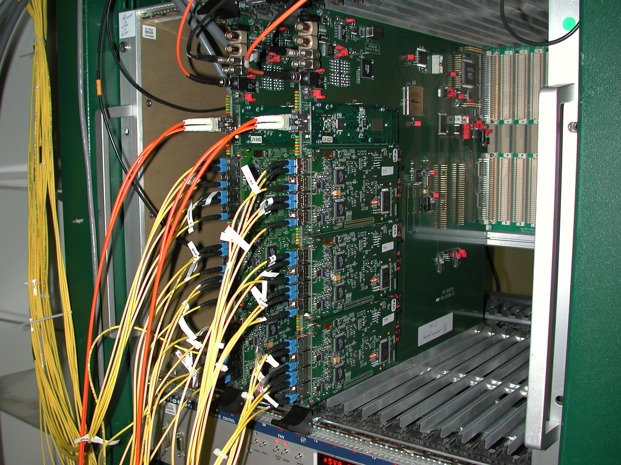
Photo gallery